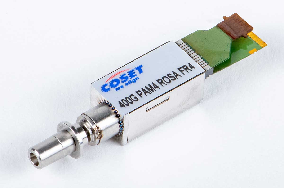
400 Gbps CWDM PAM4 ROSA FR4
All of our products are designed with attention to detail and go through a rigorous testing and quality control process from prototype to final production.
Features
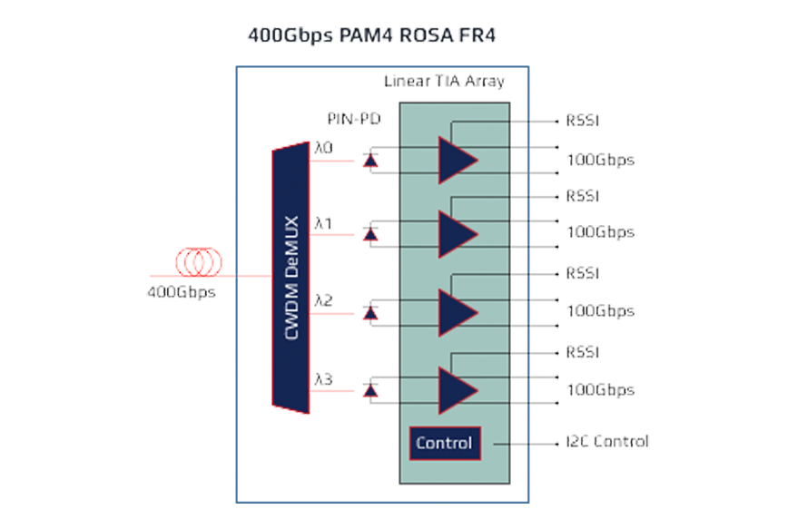
- 4 x 53GBaud CWDM 400GBASE-FR4 Ethernet
- Compatible to QSFP28 Transceivers Up to 2km
- Low Insertion Loss Optical Filter Based DEMUX
- Integrated Quad PIN-PD and Linear TIA Arrays
- Electrical Interfaces Via Separate RF and DC FPC’s
- RSSI Current Output and I2C Protocol Interface
- Optical Interface with SMF XMD-MSA LC Receptacle
Applications
- IEEE 802.3bs 400GBASE-DR4 Ethernet Application
- IEEE 802.3bs 400GBASE-FR4 Ethernet Application
- 4 x 56GBaud CWDM Transceivers
Characteristics
| PARAMETER | SYMBOL | MIN. | TYPE | MAX. | UNIT |
|---|---|---|---|---|---|
| Center Wavelengths of Channels | λcn | 1271, 1291, 1311, 1331 | nm | ||
| PD Responsivity Each Lane | R | 0.6 | 0.7 | - | A/W |
| Minimum Sensitivity Each Lane1 | SAVE | - | - | -8.8 | dBm |
| OMA Overload Each Lane1 | OLOMA | +5.2 | - | - | dBmOMA |
| Average Overload Each Lane1 | OLAVE | +5.0 | - | - | dBm |
| Small Signal Bandwidth Each Lane1,2 | BW | 30 | - | - | GHz |
| Saturated Differential Output Voltage1,3 | Vop - Von | 400 | - | - | mVp-p |
| Power Supply Voltage | Vcc | 2.9 | 3.3 | 3.5 | V |
| Power Supply Current | Icc | - | 235 | 300 | mA |
| Operating Temperature | Top | -5 | 25 | +75 | ℃ |
- Receiver sensitivity & overload of each channel without FEC is measured at 2.4×10⁻⁴ BER and PRBS 231 – 1 condition with 53 GBaud rate PAM4 signal Tx source of extinction ratio over 3.5dB.
- Average optical input power is -10dBm.
- OMA optical input power is -9dBmOMA.
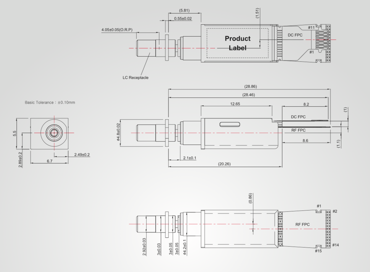
Package Specifications (Unit: mm)
Electrical Pad Configurations
| PAD # | DC FPC | RF FPC | ||
| PAD NAME | DESCRIPTION | PAD NAME | DESCRIPTION | |
| 1 | GND | Ground | GND | Ground |
| 2 | Vcc | Power Supply | GND | Ground |
| 3 | Vcc | Power Supply | D3n | Data Output (-) for L3 |
| 4 | RSSI3 | RSSI Output for L3 | D3p | Data Output (+) for L3 |
| 5 | RSSI2 | RSSI Output for L2 | GND | Ground |
| 6 | RSSI1 | RSSI Output for L1 | D2n | Data Output (-) for L2 |
| 7 | RSSI0 | RSSI Output for L0 | D2p | Data Output (+) for L2 |
| 8 | GND | Ground | GND | Ground |
| 9 | SDA | Serial Data for I2C Protocol | D1n | Data Output (-) for L1 |
| 10 | SCL | Serial Clock for I2C Protocol | D1p | Data Output (+) for L1 |
| 11 | GND | Ground | GND | Ground |
| 12 | - | - | D0n | Data Output (-) for L0 |
| 13 | - | - | D0p | Data Output (+) for L0 |
| 14 | - | - | GND | Ground |
| 15 | - | - | GND | Ground |
* Each channel from L0 to L3 is corresponding to the input signal with center wavelength of 1271, 1291, 1311, and 1331 nm respectively.
All statements, technical information and recommendations related the products herein are based upon information believed to be reliable and accurate. However, the accur acy or completeness thereof is not guaranteed, and no responsibility is assumed for any inaccuracies. The user assumes all risks and liability whatsoever in connection with the use of a product or its application. Coset Inc. reserves the right to change at any time without notice the design, specifications, function, fit or form of its products describ ed herein, including withdrawal at any time of a product offered for sales herein.


